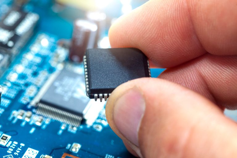
The process of creating a custom ASIC for your application will follow a predictable sequence of steps:
- Requirements Definition
- Project Sizing Analysis
- Business Case Evaluation
- Design Implementation (Phase 1)
- Design Manufacturing and Validation (Phase 2)
Requirements Definition
During this stage, the desired ASIC’s architecture, technical and physical specifications are documented, expected environmental and electrical conditions are defined, required product lifetime is documented and cost constraints are identified. The more complete the definition of requirements is at this point, the greater the chance of a successful ASIC project.
Project Sizing Analysis
During this stage, the ASIC North engineering team identifies solution options, develops a preliminary project schedule, and generates estimates for all costs such as Non-Recurring Engineering (NRE) for the development, hardware, test, characterization, and ASIC qualification.
Business Case Evaluation
During this stage we will collectively look at all aspects of the business case to see if it makes sense to move forward in a win-win fashion. There needs to be convincing evidence that the Return on Investment (ROI) is adequate and will occur in an acceptable timeframe (for both you, the customer and ASIC North).
Contact Us
Design Implementation (Phase 1)
During this stage, the target technologies are finalized for the ASIC die and package, and the ASIC is designed and verified through simulations using industry-standard EDA tools. Specific tasks can include
- analog circuit design and simulations
- digital RTL development and functional verification
- design-for-test (DFT) insertion and verification
- analog behavioral modeling and mixed-mode simulations
- custom and semi-custom layout, digital place-and-route
- static timing analysis
- test program development
- package design
Over the course of the ASIC project multiple internal and customer design reviews are conducted to compare simulated device performance to specification, to discuss how the design effort is proceeding, and to validate any assumptions made during the project sizing stage.
Once the final design review is completed, you approve moving to Phase 2, Design Manufacturing and Validation, where the ASIC is manufactured by our technology partner(s), tested, and characterized for performance against the specified requirements.
Design Manufacturing and Validation (Phase 2)
Phase 2 entails the manufacture, packaging, and validation of the ASIC. The design database is submitted to the chosen foundry for fabrication and simultaneously, work is started to prepare for device testing and characterization. This involves making packaging arrangements and creating a test environment which allows all ASIC features to be validated in silicon.
Once the ASIC silicon exits fabrication, ASIC North coordinates the packaging, initial test, and full performance characterization. A comprehensive characterization report is published and reviewed with you.
Assuming the first pass hardware meets all specified requirements, and is approved, production hardware is ordered and a plan is developed for Qualification and production ramp. The manufacturing test plan is also finalized, documented and implemented.
JEDEC standards and your requirements, drive the level of qualification that is specified. Typically device qualification is executed on finished ASIC components from several lots of production hardware in an effort to determine estimates of product lifetime.
Once device qualification is successfully completed, the ASIC design is turned over to our Supply Chain management team, who will subsequently coordinate all activities leading to fully tested components being shipped, as specified by the customer, to appropriate customers or contract manufacturers.
Check out some of our Case Studies to see examples of our Turnkey Solutions


